Patterning materials efficiently at the micrometer and nanometer scales is an essential requirement for wafer-scale semiconductor manufacturing, as well as for, e.g., display manufacturing and the production of flexible electronics. As feature sizes shrink, traditional photolithographic processes -- based on the projection of ultraviolet light -- become increasingly diffraction-limited, expensive and challenging to use. Even when spatial resolution is not a limitation, the use of photosensitive materials together with the associated deposition and etching processes may be too expensive or slow for a particular application. Increasingly, therefore, micro- and nano-scale patterning processes rely upon mechanical contact to deform materials. Some examples of these processes are nanoimprint lithography, gravure, flexography and lift-off processes that rely on controlling rate-dependent adhesion. To enable widespread industrial adoption of any of these processes, the precision and defectivity requirements that must be met are extremely challenging.
We are developing a set of numerical modeling approaches that can help to understand the physical effects at play in these mechanical patterning techniques, and how the geometrical layout of extremely complex circuit designs can be tailored to the process to enhance yield and speed of production. What these processes have in common is that the designs that are transferred are usually many orders of magnitude larger in lateral extent than the thickness of the material that is being patterned. This property makes their simulation highly amenable to the use of boundary element methods and to the use of Green's functions which encapsulate the behavior of a surface or a film of material using its deformation response to a localized load. These methods offer a highly computationally affordable way of simulating the production of chip-scale and larger designs.
Nanoimprint lithography (NIL) process modeling
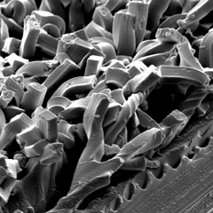
NIL is a technique in which a nanopatterned stamp, or "template" deforms a layer of thermoplastic polymer or ultraviolet-curing resin to transfer a design to a target substrate such as a silicon wafer. NIL has the potential to lower semiconductor manufacturing costs substantially, but its adoption has been hampered by a lack of understanding of how to design circuit layouts that are manufacturable using the process. NIL exhibits strong, systematic pattern dependencies: imprinting templates with large or highly varied feature sizes, shapes or densities exhibit parasitic nano-scale elastic deflections during imprinting, which propagate to damaging variation of critical device dimensions.
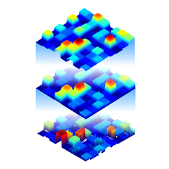
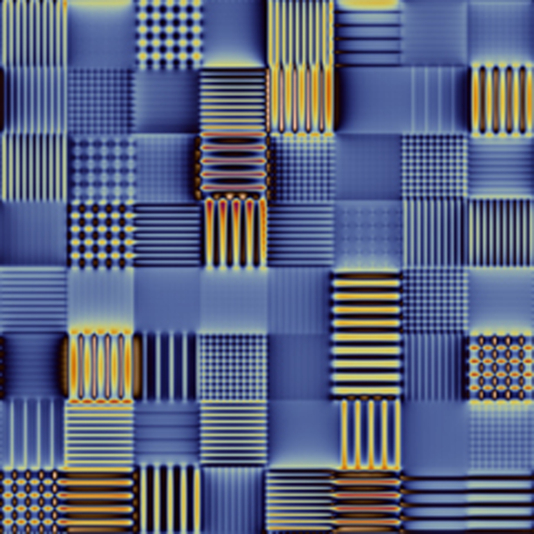
The simulation technique that we have introduced encapsulates the mechanical behavior of the imprinted polymer in an "impulse response" function. This response function is combined with an iterative algorithm to find the temporally evolving contact pressure distribution between a solid imprinting stamp and the material being deformed. From this pressure solution, the deformed shape of the polymeric material can be readily computed. The simulation approach is at least 1000 times faster than conventional mechanical simulation techniques such as finite-element modeling, and our approach enables complex chip-scale patterns to be abstracted simply. The speed of the approach means that, for the first time, numerical simulation is a feasible way of evaluating NIL for particular applications. Previously, process development has been highly experimental and iterative: engineers have tended to spend weeks tuning process parameters for a particular layout design and material set, and have faced a significant risk of needing to revise the layout design and re-make the template (at a cost often exceeding $100K) to correct for systematic defects that stem from the layout. Simulation of NIL reduces the need for this potentially wasteful effort.
The simulation technique is the subject of two issued US patents and received the 2009 Software in Design Innovation Award from the Institution of Engineering and Technology. The technology was spun out in 2010 to form Simprint Nanotechnologies, which now has customers throughout academia and industry in ten countries.
A NIL simulation engine for spun-on materials is freely available here as a command-line program that runs using Matlab Compiler Runtime.
We have developed the model to incorporate the role of the surface tension of the imprinted material in driving pattern formation, and to capture directional effects in roller-based imprint. We have also invesigated the criteria for optimally designing multi-layered elastic templates to minimize systematic pattern dependences while conforming to rough and curved substrates. Currently, we are working with the Molecular Foundry at Lawrence Berkeley National Laboratory to calibrate our model experimentally for the imprinting of UV-curing resins.
H.K. Taylor, "Defectivity prediction for droplet-dispensed UV nanoimprint lithography, enabled by fast simulation of resin flow at feature, droplet, and template scales", Proc. SPIE, vol. 9777, 97770E, Feb. 2015 (invited). doi:10.1117/12.2218757
H.K. Taylor, "Enabling layout and process optimization with fast, full-field simulation of droplet-dispensed UV-NIL", presented at Nanoimprint and Nanoprint Technology, Napa, CA, Oct. 2015 (invited). abstract .pdf | presentation .pdf
H.K. Taylor, "Fast Simulation of Pattern Formation and Process Dependencies in Roller Nanoimprint Lithography", presented at Materials Research Society Fall Meeting, Boston, MA, Nov. 2012. doi:10.1557/opl.2013.49
H.K. Taylor, "Simulation of roll-to-roll and roll-to-plate NIL: modeling the effects of process speed, imprinting load, roller elasticity, and pattern design", presented at Nanoimprint and Nanoprint Technology, Napa, CA, Oct. 2012. abstract .pdf
H.K. Taylor and E.J. Wong, "Fast simulation of nanoimprint lithography: modeling capillary pressures during resist deformation", presented at Nanoimprint and Nanoprint Technology, Jeju, Korea, Oct. 2011. abstract .pdf
D.S. Boning, A.B. Kahng, H.K. Taylor, and Y.-K. Wu, "Chip-scale simulation of residual layer thickness uniformity in thermal nanoimprint lithography: evaluating stamp cavity-height and 'dummy-fill' selection strategies", presented at Nanoimprint and Nanoprint Technology, Copenhagen, Denmark, Oct. 2010. abstract .pdf | presentation .pptx
H.K. Taylor, K. Smistrup, and D.S. Boning, "Modeling the enhancement of nanoimprint stamp bending compliance by backside grooves: mitigating the impact of wafer nanotopography on residual layer thickness", presented at Nanoimprint and Nanoprint Technology,Copenhagen, Denmark, Oct. 2010. abstract .pdf | poster .pdf
H.K. Taylor and D.S. Boning, "Towards nanoimprint lithography-aware layout design checking", Proc. SPIE, vol. 7641, 764129, 2010. doi:10.1117/12.846499 | presentation .pdf
H.K. Taylor and D.S. Boning, "Fast simulation of pattern dependencies in thermal nanoimprint lithography", presented at Nanoimprint and Nanoprint Technology, San Jose, CA, Nov. 2009. abstract .pdf | presentation .pdf
Hayden Taylor, Artos Cen